
|
시장보고서
상품코드
2044012
전력기기용 실리콘 웨이퍼 : 시장 점유율 분석, 업계 동향 및 통계, 성장 예측(2026-2031년)Silicon Wafer For Power Devices - Market Share Analysis, Industry Trends & Statistics, Growth Forecasts (2026 - 2031) |
||||||
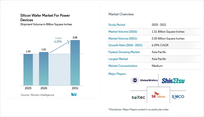
전력기기용 실리콘 웨이퍼 시장은 2025년에 14억 3,000만 평방인치로 평가되었습니다. 2026년 15억 1,000만 평방인치에서 2031년까지 20억 5,000만 평방인치에 이를 것으로 예상되며, 2026년부터 2031년까지 예측 기간에서 CAGR은 6.29%를 나타낼 전망입니다.
이러한 성장은 자동차의 전동화, 재생에너지를 통한 전력망 업그레이드, 산업용 구동 장치의 기계식 전력 제어에서 전자식 전력 제어로의 꾸준한 전환에 의해 뒷받침되고 있습니다. 와이드 밴드갭 재료, 에피택셜 장비에 대한 수출 규제 강화, 대구경 기판의 보급으로 공급망 전략이 재편되는 한편, 비용 절감 압력으로 인해 집적 장치 제조업체의 후방 통합이 진행되고 있습니다. 실리콘 웨이퍼 시장은 폴리실리콘 가격 변동으로 인해 폴리실리콘 웨이퍼의 수익률이 압박을 받고 있지만, 장기 계약으로 인해 Tier 1 공급업체에 대한 영향은 완화되고 있습니다. 300mm 라인의 규모의 경제와 북미 및 유럽의 현지화 인센티브가 결합되어 경쟁의 강도는 여전히 높은 수준입니다.
전력기기용 실리콘 웨이퍼 시장 동향과 전망
전기차 중심의 고효율 전력 변환에 대한 수요가 급증하고 있습니다.
전기자동차는 400V에서 800V 배터리 플랫폼으로 전환하고 있으며, 급속 충전 시간을 20분 이내로 단축하고 배선 무게를 줄이고 있습니다. 20kHz 이상에서 스위칭하는 SiC MOSFET은 여러 개의 실리콘 스위치를 대체하여 수동 부품의 소형화를 실현하고, 웨이퍼의 프리미엄 가격에도 불구하고 전체 인버터 비용을 절감하고 있습니다. 중국, 유럽 및 미국 자동차 제조업체들은 기판 공급을 확보하고 추가 수익을 확보하기 위해 SiC 장치 생산을 수직 통합하고 있으며, 이는 향후 몇 년 동안 웨이퍼 수요의 성장을 가속하고 있습니다. 국제에너지기구(IEA)는 2026년 배터리 전기자동차(BEV) 및 플러그인 하이브리드 자동차(PHEV)의 판매량을 1,700만대로 예측하고 있으며, 이는 약 5,000만 평방인치의 에피택셜 SiC 웨이퍼에 해당합니다. 이러한 수요는 자동차 가치사슬 전반에서 실리콘 웨이퍼 시장의 지속적인 성장을 뒷받침하고 있습니다.
재생에너지 확대가 고전압 인버터용 웨이퍼의 성장 견인
대규모 태양광 및 해상풍력 발전 설비는 1,000-1,500V의 직류 버스 전압으로 운영되고 있으며, 전력 장치의 정격 전압을 1,700V 이상으로 끌어올리고 있습니다. 2025년 미국에서는 태양광 발전 용량이 35GW, 풍력 발전 용량이 12GW 증가하며, 이는 인버터 모듈용 고전압 기판으로서 약 8,000만 평방인치에 해당합니다. 인도와 같은 신흥 시장도 연간 수 기가 와트 규모의 목표를 설정하여 이러한 추세를 따르고 있으며, 각 목표에는 SiC 디바이스를 권장하는 인버터 효율 의무화가 수반되고 있습니다. 유럽 입찰은 현재 엄격한 고조파 왜곡 임계치를 규정하여 결함 밀도가 낮은 후막 에피택셜 웨이퍼의 채택을 더욱 가속화하고 있습니다. 이러한 정책은 전반적으로 고전압 분야 실리콘 웨이퍼 시장의 모멘텀을 촉진하고 있습니다.
폴리실리콘 원료 가격 변동
폴리실리콘 현물 가격은 2023년 초 1kg당 30달러에서 2024년 말에는 1kg당 6-8달러까지 하락하여 폴리실리콘 웨이퍼의 매출 총이익률을 최대 8%까지 압박했습니다. 장기계약으로 높은 가격에 묶여있던 공급업체는 현물 구매자가 자사 가격보다 낮은 가격을 제시했을 때 기회비용을 부담해야 했습니다. 덤핑에 대한 무역 조사는 관세의 불확실성을 증가시키고, 조달 위험을 높이며, 단기적인 계획 수립을 방해했습니다. 에피택셜 등급 공급업체들은 프리미엄을 통해 어느 정도 변동성을 흡수할 수 있지만, 변동성이 지속되면 투자 의욕이 떨어지고, 비용에 민감한 부문의 웨이퍼 생산능력 증설이 지연될 수 있습니다.
부문 분석
2025년 전력기기용 실리콘 웨이퍼 시장에서 200mm 카테고리는 62.68%의 점유율을 유지했습니다. 이는 중출력 장치에서 여전히 비용 효율성이 높은 기존 팹 인프라를 반영한 것입니다. 그러나 자동차 Tier 1 공급업체들이 클린룸의 고정비를 상각하기 위해 웨이퍼당 다이 수를 늘리면서 300mm급은 CAGR 7.56%를 나타낼 것으로 예측됩니다. 초기 생산 로트에서는 동일한 결함 밀도에서 실용 가능한 다이 수가 2.3배에 달하고, 학습 곡선이 충분히 가파르기 때문에 대구경에서도 실리콘 웨이퍼 시장 규모 우위를 유지할 수 있는 것으로 확인되었습니다.
50µm을 초과하는 열기계적 휨으로 인한 수율 저하는 여전히 즉각적인 대량 채용을 제한하고 있지만, 표준화 단체는 두께 변동 목표치를 2µm 이하로 낮추도록 추진하고 있습니다. 후면 이온 주입 및 최적화된 에피택시 공정으로 두 자릿수 수율 향상을 보이고 있으며, 양산화의 전환점은 4년 이내에 도래할 것으로 예측됩니다. 뒤틀림 제어를 마스터할 수 있는 규모의 리더 기업은 실리콘 웨이퍼 시장 전체에서 지속적인 비용 우위를 유지할 수 있을 것입니다.
에피택셜 웨이퍼는 트렌치게이트 MOSFET으로의 전환을 배경으로 2025년 시장 점유율 64.39%를 차지했으며 CAGR 7.16%로 확대될 것으로 예측됩니다. 정밀한 도핑과 두께 균일성을 통해 온 저항을 낮추고 스위칭 속도를 향상시킬 수 있으며, 이는 자동차 및 재생 에너지 파워트레인에 필수적인 특성입니다. 증착 장비와 AI 지원 측정 기술의 긴밀한 협력으로 장비 가동률이 75%에서 85%까지 향상되어 프리미엄 부문의 실리콘 웨이퍼 시장의 견조한 규모를 뒷받침할 수 있는 잠재적 생산 능력을 확보할 수 있게 되었습니다.
연마 기판은 다이오드 및 기존 사이리스터에서 여전히 중요한 역할을 하고 있습니다. 이들 분야는 가격 문턱은 낮지만 폴리실리콘 가격의 급등으로 인해 수익률에 대한 압박이 커지고 있습니다. 연마 및 에피택셜 부문에서 사업을 운영하는 공급업체는 위험을 효과적으로 완화할 수 있습니다. 그러나 지속적인 성장은 분명히 고사양 에피택시로 이동하고 있으며, 이는 광범위한 실리콘 웨이퍼 시장에서의 전략적 중요성을 강조하고 있습니다.
"전력기기용 실리콘 웨이퍼 시장 보고서는 직경(150mm 이상), 웨이퍼 유형(연마 및 에피택셜), 디바이스 유형(IGBT 등), 전압 범위(저전압, 중전압, 고전압), 최종 사용 산업(자동차, 산업 및 자동화, 재생에너지 및 에너지 저장 등), 지역별로 분류되어 있습니다. 에너지 저장 등) 및 지역별로 분류되어 있습니다. 시장 예측은 수량(평방인치) 기준으로 제공됩니다.
지역별 분석
아시아태평양은 2025년 시장 점유율의 69.98%를 차지했으며 2031년까지 연평균 복합 성장률(CAGR) 8.01%를 나타낼 것으로 예측됩니다. 중국의 '국가 실리콘 산업 그룹'의 확장 계획, 일본의 300mm 연마 라인 투자, 한국의 SiC 생산 능력 증설은 실리콘 웨이퍼 시장을 뒷받침하는 견고한 생태계를 형성하고 있습니다. 정부의 로봇 공학, EV, 재생에너지에 대한 목표는 지역 수요를 더욱 강화하여 현지 팹이 거의 풀가동 상태를 유지할 수 있도록 보장합니다.
북미에서는 'CHIPS법'의 인센티브와 자동차 산업의 현지화 목표를 계기로 투자가 급증하고 있습니다. 뉴욕, 노스캐롤라, 텍사스에 신설되는 시설은 수입 의존도를 낮추고 공급 리스크를 분산하는 한편, 최첨단 300mm 공정을 최종 시장과 가까운 곳에 정착시킬 것입니다. 이 지역의 정책적 환경과 주요 반도체 제조 장비 공급업체에 대한 접근성을 결합하여 실리콘 웨이퍼 시장에서 유력한 제2의 거점으로 자리매김하고 있습니다.
유럽은 유럽 칩 법과 엄격한 자동차 배기가스 규제를 활용하여 세계 파워 디바이스 생산에서 점유율을 확대되고 있습니다. 독일과 이탈리아의 확장 프로젝트는 수십억 달러 규모의 공공 자금으로 지원되며, SiC 에피택시와 300mm 실리콘에 중점을 두고 있습니다. 엔지니어드 서브스트레이트와 초박형 웨이퍼에 특화된 공동 플랫폼은 비용 리더십이 아닌 기술 차별화를 추구하는 유럽의 전략을 여실히 보여주고 있습니다. 남미, 중동 및 아프리카는 여전히 수입에 의존하고 있는 상황이지만, 초기 노력으로 볼 때, 이 지역에 서브 스트레이트 제조 역량을 구축하려는 장기적인 야심을 엿볼 수 있습니다.
기타 혜택 :
- 엑셀 형식 시장 예측(ME) 시트
- 3개월간 애널리스트 지원
자주 묻는 질문
목차
제1장 서론
제2장 조사 방법
제3장 주요 요약
제4장 시장 구도
제5장 시장 규모와 성장 예측
제6장 경쟁 구도
제7장 시장 기회와 향후 전망
KTH 26.05.29The silicon wafer market for power devices was valued at 1.43 billion square inches in 2025 and is estimated to grow from 1.51 billion square inches in 2026 to reach 2.05 billion square inches by 2031, at a 6.29% CAGR during the forecast period from 2026 to 2031.

Growth is anchored by vehicle electrification, renewable-energy grid upgrades, and the steady conversion of industrial drives from mechanical to electronic power control. Wide-bandgap materials, tighter export rules on epitaxial tools, and larger-diameter substrates are reshaping supply-chain strategies, while cost-reduction pressure is encouraging backward integration by integrated device manufacturers. The silicon wafer market is further influenced by polysilicon price swings that compress polished-wafer margins, although long-term contracts soften the impact for tier-one suppliers. Competitive intensity remains high as scale advantages in 300 mm lines converge with localization incentives in North America and Europe.
Insights and Trends of Silicon Wafer Market For Power Devices
EV-Led Demand Surge for High-Efficiency Power Conversion
Electric vehicles are shifting from 400-volt to 800-volt battery platforms, cutting fast-charge times to under 20 minutes and reducing wiring mass. SiC MOSFETs switching above 20 kHz replace multiple silicon switches, shrinking passive components and lowering total inverter cost even at a wafer premium. Automakers in China, Europe, and the United States are vertically integrating SiC device production to secure substrate supply and capture additional margin, reinforcing multi-year wafer demand growth. The International Energy Agency projects battery-electric and plug-in hybrid sales of 17 million units in 2026, which equates to roughly 50 million square inches of epitaxial SiC wafers. This demand underpins sustained expansion of the silicon wafer market across the automotive value chain.
Renewable-Energy Build-Out Driving High-Voltage Inverter Wafers
Utility-scale solar and offshore wind installations operate at direct-current bus voltages between 1,000 and 1,500 volts, pushing power-device ratings beyond 1,700 volts. In 2025 the United States added 35 GW of solar and 12 GW of wind capacity, translating into nearly 80 million square inches of high-voltage substrates for inverter modules. Emerging markets such as India are matching this trajectory through multi-gigawatt annual targets, each paired with inverter efficiency mandates that favor SiC devices. European auctions now stipulate stringent harmonic-distortion thresholds, further accelerating the adoption of thick-epi wafers with low defect densities. These policies collectively reinforce the silicon wafer market's momentum in high-voltage segments.
Polysilicon Feedstock Price Volatility
Spot polysilicon prices fell from USD 30 per kg in early 2023 to USD 6-8 per kg by late 2024, compressing polished-wafer gross margins by up to eight percentage points. Suppliers locked into higher long-term contracts faced opportunity costs when spot buyers undercut their pricing. Trade investigations on dumping added tariff uncertainty, raising procurement risk and hindering short-term planning. Although epitaxial-grade suppliers can absorb some variance through premiums, sustained volatility dampens investment appetite and can slow wafer-capacity additions in cost-sensitive segments.
Other drivers and restraints analyzed in the detailed report include:
- Shift to 300 mm Lines Lowering Cost Per Die
- Rising Industrial Automation and Electrified Factory Drives
- USD 1 Billion+ CAPEX Barrier for 200-300 mm SiC Wafer Fabs
For complete list of drivers and restraints, kindly check the Table Of Contents.
Segment Analysis
The 200 mm category retained 62.68% of the silicon wafer market for power devices in 2025, reflecting legacy fab infrastructure that remains cost-effective for medium-power devices. Yet the 300 mm class is forecast to post a 7.56% CAGR as automotive tier-ones demand larger die counts per wafer to amortize clean-room overhead. Early production runs already demonstrate 2.3-times usable die with comparable defect density, confirming that learning curves are steep enough to sustain the silicon wafer market size advantages at larger diameters.
Yield drag from thermo-mechanical bow above 50 µm still limits immediate mass adoption, but standards groups are driving thickness-variation targets below 2 µm. Back-side ion implantation and optimized epitaxy recipes are showing double-digit yield gains, suggesting that volume tipping points will arrive within four years. Scale leaders able to master bow control will hold durable cost positions across the silicon wafer market.
Epitaxial wafers captured 64.39% of the market share in 2025 on the strength of trench-gate MOSFET migration, and they are set to advance at a 7.16% CAGR. Precise doping and thickness uniformity enable lower on-resistance and higher switching speeds, attributes essential to automotive and renewable-energy power trains. Tight integration between deposition tools and AI-assisted metrology now lifts tool utilization from 75% to 85%, freeing latent capacity that underpins a resilient silicon wafer market size at the premium end.
Polished substrates remain relevant in diodes and legacy thyristors, where value thresholds are low but margin pressure is increasing due to polysilicon price shocks. Suppliers operating in both polished and epitaxial segments mitigate risks effectively. However, sustained growth is clearly shifting toward high-specification epitaxy, emphasizing its strategic importance within the broader silicon wafer market.
The Silicon Wafer Market for Power Devices Report is Segmented by Diameter (150 Mm, and More), Wafer Type (Polished, and Epitaxial), Device Type (IGBT, and More), Voltage Range (Low Voltage, Medium Voltage, and High Voltage), End-Use Industry (Automotive, Industrial and Automation, Renewable Energy and Energy Storage, and More), and Geography. The Market Forecasts are Provided in Terms of Volume (Square Inches).
Geography Analysis
Asia-Pacific commanded 69.98% of the market share in 2025 and is projected to post an 8.01% CAGR through 2031. Expansion programs by China's National Silicon Industry Group, Japan's investments in 300 mm polishing lines, and South Korea's SiC capacity additions create a formidable ecosystem that anchors the silicon wafer market. Government robotics, EV, and renewable-energy targets further reinforce regional demand, ensuring that local fabs operate near full utilization.
North America is experiencing an investment surge catalyzed by CHIPS Act incentives and automotive localization goals. New facilities in New York, North Carolina, and Texas reduce dependence on imports, diversify supply risk, and embed advanced 300 mm processes closer to end-markets. The region's policy environment, combined with access to leading semiconductor equipment suppliers, positions it as a credible secondary hub in the silicon wafer market.
Europe leverages the European Chips Act and stringent vehicle-emission rules to claim a larger share of global power-device production. Expansion projects in Germany and Italy emphasize SiC epitaxy and 300 mm silicon, supported by multi-billion-dollar public funding. Collaborative platforms focused on engineered substrates and ultra-thin wafers illustrate Europe's strategy of technology differentiation rather than cost leadership. South America and the Middle East and Africa remain import-oriented today, yet early initiatives signal long-term ambitions to establish regional substrate capabilities.
- Shin-Etsu Chemical
- SUMCO Corporation
- GlobalWafers Co., Ltd.
- Siltronic AG
- SK Siltron Co., Ltd.
- Soitec S.A.
- National Silicon Industry Group (NSIG)
- Wafer Works Corporation
- Ferrotec Holdings Corporation
- Hangzhou Lion Microelectronics
- Infineon Technologies AG
- STMicroelectronics N.V.
- onsemi
- Wolfspeed, Inc.
- ROHM Co., Ltd.
- Mitsubishi Electric Corporation
- Fuji Electric Co., Ltd.
- SKC-TankeBlue Semiconductor
- Showa Denko K.K.
- Hebei Synlight Crystal
Additional Benefits:
- The market estimate (ME) sheet in Excel format
- 3 months of analyst support
TABLE OF CONTENTS
1 INTRODUCTION
- 1.1 Study Assumptions and Market Definition
- 1.2 Scope of the Study
2 RESEARCH METHODOLOGY
3 EXECUTIVE SUMMARY
4 MARKET LANDSCAPE
- 4.1 Market Overview
- 4.2 Market Drivers
- 4.2.1 EV-Led Demand Surge for High-Efficiency Power Conversion
- 4.2.2 Renewable-Energy Build-Out Driving High-Voltage Inverter Wafers
- 4.2.3 Shift to 300 Mm Lines Lowering Cost Per Die
- 4.2.4 Rising Industrial Automation and Electrified Factory Drives
- 4.2.5 On-Wafer Back-Side Vias Enabling Ultra-Thin Automotive Modules
- 4.2.6 AI-Driven In-Situ Metrology Freeing Latent Epi Capacity
- 4.3 Market Restraints
- 4.3.1 Polysilicon Feedstock Price Volatility
- 4.3.2 USD 1 B+ CAPEX Barrier for 200-300 Mm Sic Wafer Fabs
- 4.3.3 Thermo-Mechanical Bow in 300 Mm Sic Wafers Slashing Yields
- 4.3.4 Export-Control Uncertainty for Next-Gen Epi Reactors
- 4.4 Industry Supply-Chain Analysis
- 4.5 Regulatory Landscape
- 4.6 Technological Outlook
- 4.7 Impact of Macroeconomic Factors on the Market
- 4.8 Porter's Five Forces Analysis
- 4.8.1 Threat of New Entrants
- 4.8.2 Bargaining Power of Suppliers
- 4.8.3 Bargaining Power of Buyers
- 4.8.4 Threat of Substitutes
- 4.8.5 Intensity of Competitive Rivalry
5 MARKET SIZE AND GROWTH FORECASTS (VOLUME)
- 5.1 By Diameter
- 5.1.1 150 mm
- 5.1.2 200 mm
- 5.1.3 300 mm
- 5.2 By Wafer Type
- 5.2.1 Polished
- 5.2.2 Epitaxial
- 5.3 By Device Type
- 5.3.1 IGBT
- 5.3.2 MOSFET
- 5.3.3 Diode
- 5.3.4 Thyristor
- 5.4 By Voltage Range
- 5.4.1 Low Voltage (Less than 200V)
- 5.4.2 Medium Voltage (200-650V)
- 5.4.3 High Voltage (Above 650V)
- 5.5 By End-Use Industry
- 5.5.1 Automotive
- 5.5.2 Industrial and Automation
- 5.5.3 Renewable Energy and Energy Storage
- 5.5.4 Consumer and Appliance Power
- 5.5.5 Telecom and Infrastructure Power Systems
- 5.6 By Geography
- 5.6.1 North America
- 5.6.1.1 United States
- 5.6.1.2 Canada
- 5.6.1.3 Mexico
- 5.6.2 Europe
- 5.6.2.1 Germany
- 5.6.2.2 United Kingdom
- 5.6.2.3 France
- 5.6.2.4 Rest of Europe
- 5.6.3 Asia-Pacific
- 5.6.3.1 China
- 5.6.3.2 Japan
- 5.6.3.3 India
- 5.6.3.4 South Korea
- 5.6.3.5 Taiwan
- 5.6.3.6 Rest of Asia-Pacific
- 5.6.4 South America
- 5.6.5 Middle East and Africa
- 5.6.1 North America
6 COMPETITIVE LANDSCAPE
- 6.1 Market Concentration
- 6.2 Strategic Moves
- 6.3 Market Share Analysis
- 6.4 Company Profiles (includes Global level Overview, Market Level Overview, Core Segments, Financials as Available, Strategic Information, Market Rank/Share for Key Companies, Products and Services, and Recent Developments)
- 6.4.1 Shin-Etsu Chemical
- 6.4.2 SUMCO Corporation
- 6.4.3 GlobalWafers Co., Ltd.
- 6.4.4 Siltronic AG
- 6.4.5 SK Siltron Co., Ltd.
- 6.4.6 Soitec S.A.
- 6.4.7 National Silicon Industry Group (NSIG)
- 6.4.8 Wafer Works Corporation
- 6.4.9 Ferrotec Holdings Corporation
- 6.4.10 Hangzhou Lion Microelectronics
- 6.4.11 Infineon Technologies AG
- 6.4.12 STMicroelectronics N.V.
- 6.4.13 onsemi
- 6.4.14 Wolfspeed, Inc.
- 6.4.15 ROHM Co., Ltd.
- 6.4.16 Mitsubishi Electric Corporation
- 6.4.17 Fuji Electric Co., Ltd.
- 6.4.18 SKC-TankeBlue Semiconductor
- 6.4.19 Showa Denko K.K.
- 6.4.20 Hebei Synlight Crystal
7 MARKET OPPORTUNITIES AND FUTURE OUTLOOK
- 7.1 White-space and Unmet-Need Assessment
