
|
시장보고서
상품코드
2044016
산업용 반도체 실리콘 웨이퍼 : 시장 점유율 분석, 업계 동향 및 통계, 성장 예측(2026-2031년)Industrial Semiconductor Silicon Wafer - Market Share Analysis, Industry Trends & Statistics, Growth Forecasts (2026 - 2031) |
||||||
산업용 반도체 실리콘 웨이퍼 시장 규모는 2025년 20억 3,000만 평방인치로 평가되었습니다. 2026년 21억 평방인치로부터, 2031년까지 25억 5,000만 평방인치로 확대되며 2026년부터 2031년까지 연평균 복합 성장률(CAGR)은 3.98%를 나타낼 전망입니다.

증가분의 대부분은 이미 전체 소비량의 절반을 차지하고 있는 300mm 기판에 의한 것이지만, 실리콘 카바이드(SiC) 파워 디바이스용 200mm 에피택셜 웨이퍼와 포토닉스용 실리콘 온 인슐레이터(SOI) 웨이퍼도 점유율 확대에 박차를 가하고 있습니다. 하고 있습니다. 메모리 분야 투자 회복, 게이트 올 어라운드(GAA) 로직에 대한 평탄도 요건 강화, 2025년 재고 정상화 등이 결합되어 출하 모멘텀을 촉진하고 있습니다. 중국의 사상 최고 수준의 웨이퍼 투자, 유럽공급망 복원력 강화 노력, 그리고 미국의 CHIPS 법에 따른 보조금 제도가 생산 능력 결정을 재구성하고 있으며, 많은 경우 순수한 비용 측면의 고려사항보다 더 큰 영향을 미치고 있습니다. 헬륨 가격의 급등, 200mm용 장비의 노후화 및 포장으로 인한 뒤틀림은 여전히 주요 운영 위험 요소로 남아 있습니다. 한편, 기존 기업들은 AI를 활용한 결정 성장 제어 및 리클레임(재사용) 노력을 활용하여 비용 압박에 대응하고 수익률을 유지하고 있습니다.
세계의 산업용 반도체 실리콘 웨이퍼 시장 동향과 인사이트
전기차 보급 확대와 800V 차량 플랫폼으로의 전환
배터리 전기자동차(BEV) 모델은 400V 시스템에서 800V 시스템으로 전환하고 있습니다. 이를 통해 충전 시간을 단축하고 배선 무게를 줄일 수 있지만, 200mm 에피택셜 웨이퍼에서 제조된 SiC MOSFET이 필요합니다. 인피니언은 2024년 AI를 통한 결정 성장 공정 최적화를 통해 200mm SiC 수율을 약 85% 향상시켜 설비투자를 비례적으로 늘리지 않고도 생산량을 두 배로 늘릴 수 있게 되었습니다. Wolfspeed는 같은 해에 200mm SiC 웨이퍼의 비용을 30% 절감하여 기존 실리콘 소자와의 가격 차이를 확대했습니다. 중국의 BYD와 NIO는 일찌감치 800V를 채택하여 국내 기판 공급을 확보하는 한편, 세계 리드타임을 26주 이상으로 늘렸습니다. 따라서, 200mm 웨이퍼공급 부족은 단순한 주기적인 재고 문제가 아니라 EV로의 전환에 따른 결과라고 할 수 있습니다.
800V 충전 인프라의 신속한 정비
유럽의 '대체연료 인프라 규제'는 2025년까지 주요 간선도로를 따라 60km마다 고출력 충전기를 설치하도록 의무화하고 있으며, 이에 따라 2024년부터 2025년까지 5만 개 이상의 초고속 충전시설이 설치되었습니다. 중국 국가 전력망은 2025년에 10만 개 이상의 새로운 350kW 충전 포트를 가동했으며, 각 전력 모듈에는 여러 개의 SiC 또는 GaN 다이가 장착되어 있습니다. ABB와 같은 충전 장비 제조업체들은 공급을 확보하기 위해 200mm 웨이퍼의 다년 계약을 체결하고 있으며, 이로 인해 현물 시장이 더욱 타이트해져 수요 전망은 더욱 밝아지고 있습니다.
200mm 기판 공급 부족
장비 제조업체는 200mm 장비의 신규 개발을 거의 동결하고 있기 때문에 팹은 리드 타임이 긴 재생 라인에 의존할 수밖에 없어 구조적인 공급 부족이 고착화되어 있습니다. 옥메틱이 핀란드에서 5만장 분량의 웨이퍼 생산능력을 늘린다고 해도 세계 수요의 2% 미만에 불과하며, 자동차 업계의 26주 대기시간을 완화할 수 없습니다. 대형 IDM들이 아날로그 워크로드를 300mm로 전환하는 가운데, 틈새 업체들은 더욱 까다로운 과제에 직면해 있습니다.
부문 분석
산업용 반도체 실리콘 웨이퍼 시장 규모 중 300mm가 차지하는 비중은 2025년 48.62%를 나타냈으며, 주요 로직 및 메모리 팹이 패스당 다이 수를 늘리면서 CAGR 4.85%를 나타낼 것으로 예측됩니다. Samsung Electronics와 SK하이닉스는 2026년 DRAM 생산 개시 물량의 5분의 1 이상을 고 대역폭 메모리에 할당해 300mm 블랭크 웨이퍼의 소비를 가속화하고 있습니다. 아날로그 IDM도 200mm의 병목현상을 피하기 위해 300mm로의 전환을 고려하고 있습니다.
기존 장비로 충분하고 설비투자가 적은 RF, 센서, 광전자 분야에서는 여전히 소구경 웨이퍼에 대한 수요가 존재합니다. 그러나 하이브리드 본딩 및 TSV(실리콘 관통 전극) 패키징은 300mm 기판에서만 달성할 수 있는 평탄도 공차를 요구하기 때문에 많은 첨단 프로젝트가 사실상 대구경 포맷에 묶여 있습니다. National Silicon Industry Group을 필두로 한 중국 공급업체들은 범용 300mm급에 새로운 자금을 투입하고 있으며,월100만장 이상의 웨이퍼를 공급하며 일본의 지배적 지위에 도전하고 있습니다.
'산업용 반도체 실리콘 웨이퍼 시장 보고서'는 웨이퍼 직경(150mm 이하, 200mm, 300mm), 반도체 소자 유형(로직, 메모리, 아날로그 등), 웨이퍼 유형(프라임 폴리싱, 에피택셜, SOI, 특수 실리콘), 지역(북미, 유럽, 아시아, 아시아태평양, 남미, 중동, 아프리카) 태평양, 남미, 중동/아프리카)로 분류되어 있습니다. 시장 예측은 수량(평방인치) 단위로 제공됩니다.
지역별 분석
2025년 아시아태평양은 세계 소비량의 82.39%를 차지했으며 4.15%의 연평균 복합 성장률(CAGR)을 유지하여 산업용 반도체 실리콘 웨이퍼 시장에서 확고한 선두를 유지할 것으로 예측됩니다. 중국만 해도 2025년 상반기에만 4,550억 위안(633억 달러)을 투자해 전면 생산능력을 확충했으며, 그중 절반 이상을 기판에 투자했습니다. 대만은 최첨단 로직, 한국은 메모리, 일본은 광대역 갭 및 SOI 파일럿 라인에 집중하고 있습니다.
북미는 여전히 규모는 작지만, CHIPS법 자금이 GlobalWafers의 35억 달러 규모의 텍사스 공장에 힘을 실어주었고, 같은 해에 40억 달러 규모의 추가 확장을 발표하는 등 빠르게 성장하고 있습니다. SK실트론의 미시간 공장은 36억 달러의 예산이 책정되어 있으며, 2027년까지 300mm의 새로운 생산능력을 갖출 예정입니다. 캐나다와 멕시코는 백엔드 공정을 담당하고 있으며, 이는 재생 웨이퍼와 테스트용 웨이퍼 수요를 견인하고 있습니다.
유럽은 430억 유로(473억 달러) 규모의 CHIPS법을 통해 점유율을 안정화시키고 있으며, 실트로닉이 싱가포르에 건설하는 20억 유로(22억 달러) 규모의 'Fab-Next'를 지원하여 두 지역에 걸친 고객들을 지원하고 있습니다. 독일과 프랑스는 아날로그 및 파워 반도체의 자급자족을 중시하고 있으며, 전 세계가 300mm로 전환하는 와중에도 200mm의 중요성을 유지하고 있습니다. 기타 지역은 모두 합쳐도 2% 미만의 점유율에 불과하지만, 재생에너지에 대한 의지와 연계된 SiC(탄화규소) 관련 사업을 모색하고 있습니다.
기타 혜택 :
- 엑셀 형식 시장 예측(ME) 시트
- 3개월간 애널리스트 지원
자주 묻는 질문
목차
제1장 서론
제2장 조사 방법
제3장 주요 요약
제4장 시장 구도
제5장 시장 규모와 성장 예측
제6장 경쟁 구도
제7장 시장 기회와 향후 전망
KTH 26.05.29The industrial semiconductor silicon wafer market size is projected to expand from 2.03 billion square inches in 2025 and 2.10 billion square inches in 2026 to 2.55 billion square inches by 2031, registering a CAGR of 3.98% between 2026 and 2031.
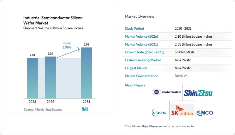
Most of the incremental area will come from 300 mm substrates, which already account for nearly half of total consumption, while 200 mm epitaxial wafers for silicon-carbide (SiC) power devices and silicon-on-insulator (SOI) wafers for photonics accelerate their mix gains. A rebound in memory spending, tighter flatness requirements for gate-all-around logic, and inventory normalization in 2025 have together lifted shipment momentum. China's record wafer investments, Europe's push for supply-chain resilience, and the United States' CHIPS Act subsidies are reshaping capacity decisions, often overriding pure cost considerations. Helium price spikes, 200 mm tool obsolescence, and packaging-induced warpage remain the chief operational risks. Meanwhile, incumbents use AI-based crystal-growth controls and reclaim initiatives to offset cost pressure and preserve margins.
Global Industrial Semiconductor Silicon Wafer Market Trends and Insights
Rising EV Penetration And Shift Toward 800-V Vehicle Platforms
Battery-electric models are migrating from 400-V to 800-V systems, which cuts charging time and wiring weight, but requires SiC MOSFETs processed on 200 mm epitaxial wafers. Infineon boosted 200 mm SiC yields by nearly 85% in 2024 through AI-optimized crystal growth, letting the firm double output without proportional capex. Wolfspeed achieved a 30% cost reduction in 200 mm SiC wafers that same year, widening the price gap with legacy silicon devices. Chinese brands BYD and NIO adopted 800 V early, locking in domestic substrate supply and extending global lead times beyond 26 weeks. Tight 200 mm availability is therefore an outgrowth of the EV transition and not merely a cyclical inventory issue.
Rapid Build-Out Of 800 V Charging Infrastructure
The European Alternative Fuels Infrastructure Regulation mandates high-power chargers every 60 km along core corridors by 2025, triggering more than 50,000 ultra-fast installations in 2024-2025.China's State Grid commissioned over 100,000 new 350 kW ports in 2025, each power module containing multiple SiC or GaN die. Charging-equipment makers such as ABB sign multiyear 200 mm wafer contracts to protect supply, further straining the spot market and reinforcing demand visibility.
Limited Availability Of 200 MM Substrates
Toolmakers have largely frozen new 200 mm equipment development, so fabs depend on refurbished lines with longer lead times, locking in a structural shortage. Okmetic's 50,000-wafer capacity addition in Finland adds less than 2% to global demand and fails to ease 26-week automotive waits. As large IDMs migrate analog workloads to 300 mm, niche players face even tighter allocations.
Other drivers and restraints analyzed in the detailed report include:
- High-Temperature, High-Frequency Advantages Over Silicon
- Government Incentives For Wide-Band-Gap Fabs
- Capital-Intensive Crystal-Growth Equipment
For complete list of drivers and restraints, kindly check the Table Of Contents.
Segment Analysis
The 300 mm portion of the industrial semiconductor silicon wafer market size commanded 48.62% in 2025 and is on track for a 4.85% CAGR as leading logic and memory fabs seek larger die counts per pass. Samsung and SK Hynix dedicated more than one-fifth of their DRAM starts to high-bandwidth memory in 2026, accelerating consumption of 300 mm blanks. Even analog IDMs now explore 300 mm conversions to escape 200 mm bottlenecks.
Smaller diameters retain relevance in RF, sensors, and optoelectronics where legacy tools suffice and capex is modest. However, hybrid bonding and through-silicon-via packaging demand the flatness tolerance achievable only on 300 mm substrates, effectively locking many advanced programs into the larger format. Chinese suppliers, led by National Silicon Industry Group, funnel fresh funding into commodity 300 mm grades, adding over 1 million wafers a month and challenging Japanese dominance.
The Industrial Semiconductor Silicon Wafer Market Report is Segmented by Wafer Diameter (Up To 150 Mm, 200 Mm, and 300 Mm), Semiconductor Device Type (Logic, Memory, Analog, and More), Wafer Type (Prime Polished, Epitaxial, SOI, and Specialty Silicon), and Geography (North America, Europe, Asia-Pacific, South America, Middle East, Africa). The Market Forecasts are Provided in Terms of Volume (Square Inches).
Geography Analysis
Asia-Pacific represented 82.39% of worldwide consumption in 2025, and its 4.15% CAGR keeps the region firmly atop the industrial semiconductor silicon wafer market. China alone spent CNY 455 billion (USD 63.3 billion) on front-end capacity in 1H 2025, funneling more than half into substrates. Taiwan focuses on leading-edge logic, South Korea on memory, and Japan on wide-band-gap and SOI pilot lines.
North America remains smaller but grows quickly as CHIPS Act money underwrites GlobalWafers' USD 3.5 billion Texas fab, with an additional USD 4 billion expansion announced the same year. SK Siltron's Michigan site, budgeted at USD 3.6 billion, will bring fresh 300 mm capacity by 2027. Canada and Mexico handle backend steps, which in turn drive demand for reclaimed or test wafers.
Europe stabilizes its share through the EUR 43 billion (USD 47.3 billion) Chips Act, supporting Siltronic's EUR 2 billion (USD 2.2 billion) Fab-Next in Singapore for dual-region customers. Germany and France emphasize analog and power sovereignty, prolonging 200 mm relevance despite global 300 mm migration. Other regions together hold under 2% share but explore SiC initiatives tied to renewable power ambitions.
- Shin-Etsu Chemical Co., Ltd.
- SUMCO Corporation
- GlobalWafers Co., Ltd.
- Siltronic AG
- SK Siltron Co., Ltd.
- Soitec SA
- Okmetic Oy
- Wafer Works Corp.
- National Silicon Industry Group (NSIG)
- Zhonghuan Advanced Semiconductor Materials
- QL Electronics
- Nanjing Guosheng Electronics
- Hebei Puxing Electronic Technology
- Shanghai Advanced Silicon Technology (AST)
- Ferrotec Holdings Corporation
- Topsil Semiconductor Materials
- Retain GlobalWafers Co.,
- Simgui
- GRINM Semiconductor Materials
- ESWIN Technology Group
- Formosa Sumco Technology Corp.
Additional Benefits:
- The market estimate (ME) sheet in Excel format
- 3 months of analyst support
TABLE OF CONTENTS
1 INTRODUCTION
- 1.1 Study Assumptions and Market Definition
- 1.2 Scope of the Study
2 RESEARCH METHODOLOGY
3 EXECUTIVE SUMMARY
4 MARKET LANDSCAPE
- 4.1 Market Overview
- 4.2 Industry Value-Chain Analysis
- 4.3 Regulatory Landscape
- 4.4 Technological Outlook
- 4.5 Impact of Macroeconomic Factors on the Market
- 4.6 Porter's Five Forces Analysis
- 4.6.1 Bargaining Power of Suppliers
- 4.6.2 Bargaining Power of Buyers
- 4.6.3 Threat of New Entrants
- 4.6.4 Threat of Substitutes
- 4.6.5 Intensity of Competitive Rivalry
- 4.7 Market Drivers
- 4.7.1 Rising EV Penetration and Shift Toward 800-V Vehicle Platforms
- 4.7.2 Rapid Build-Out of 800 V Charging Infrastructure
- 4.7.3 High-Temperature, High-Frequency Performance Advantages over Si
- 4.7.4 Government Incentives for Wide-Band-Gap Fabs
- 4.7.5 AI-Driven Demand for 3D-IC Silicon Photonics Requiring Ultra-Flat SOI Wafers
- 4.7.6 Wafer Reclaim And Circular-Economy Mandates Lowering Total Cost-of-Ownership for 300 mm Lines
- 4.8 Market Restraints
- 4.8.1 Limited Availability of 200 mm Substrates
- 4.8.2 Capital-Intensive Crystal-Growth Equipment
- 4.8.3 Packaging-Induced Thermo-Mechanical Stress
- 4.8.4 Looming Helium Supply Constraints Impacting CMP and Epitaxial Tools
5 MARKET SIZE And GROWTH FORECASTS (VOLUME)
- 5.1 By Wafer Diameter
- 5.1.1 Up to 150 mm
- 5.1.2 200 mm
- 5.1.3 300 mm
- 5.2 By Semiconductor Device Type
- 5.2.1 Logic
- 5.2.2 Memory
- 5.2.3 Analog
- 5.2.4 Discrete
- 5.2.5 Other Semiconductor Device Types (Optoelectronics, Sensors, Micro)
- 5.3 By Wafer Type
- 5.3.1 Prime Polished
- 5.3.2 Epitaxial
- 5.3.3 Silicon-on-Insulator (SOI)
- 5.3.4 Specialty Silicon (High-Resistivity, Power, Sensor-Grade)
- 5.4 By Geography
- 5.4.1 North America
- 5.4.1.1 United States
- 5.4.1.2 Canada
- 5.4.1.3 Mexico
- 5.4.2 Europe
- 5.4.2.1 Germany
- 5.4.2.2 United Kingdom
- 5.4.2.3 France
- 5.4.2.4 Rest of Europe
- 5.4.3 Asia-Pacific
- 5.4.3.1 China
- 5.4.3.2 Japan
- 5.4.3.3 India
- 5.4.3.4 South Korea
- 5.4.3.5 Taiwan
- 5.4.3.6 Rest of Asia-Pacific
- 5.4.4 South America
- 5.4.5 Middle East
- 5.4.6 Africa
- 5.4.1 North America
6 COMPETITIVE LANDSCAPE
- 6.1 Market Concentration
- 6.2 Strategic Moves
- 6.3 Market Share Analysis
- 6.4 Company Profiles (includes Global Level Overview, Market Level Overview, Core Segments, Financials as available, Strategic Information, Market Rank/Share, Products And Services, Recent Developments)
- 6.4.1 Shin-Etsu Chemical Co., Ltd.
- 6.4.2 SUMCO Corporation
- 6.4.3 GlobalWafers Co., Ltd.
- 6.4.4 Siltronic AG
- 6.4.5 SK Siltron Co., Ltd.
- 6.4.6 Soitec SA
- 6.4.7 Okmetic Oy
- 6.4.8 Wafer Works Corp.
- 6.4.9 National Silicon Industry Group (NSIG)
- 6.4.10 Zhonghuan Advanced Semiconductor Materials
- 6.4.11 QL Electronics
- 6.4.12 Nanjing Guosheng Electronics
- 6.4.13 Hebei Puxing Electronic Technology
- 6.4.14 Shanghai Advanced Silicon Technology (AST)
- 6.4.15 Ferrotec Holdings Corporation
- 6.4.16 Topsil Semiconductor Materials
- 6.4.17 Retain GlobalWafers Co.,
- 6.4.18 Simgui
- 6.4.19 GRINM Semiconductor Materials
- 6.4.20 ESWIN Technology Group
- 6.4.21 Formosa Sumco Technology Corp.
7 MARKET OPPORTUNITIES AND FUTURE OUTLOOK
- 7.1 White-Space and Unmet-Need Assessment
