
|
시장보고서
상품코드
2063438
GaN-on-사파이어 LED 에피텍셜 웨이퍼 시장 : 점유율 분석, 업계 동향과 통계, 성장 예측(2026-2031년)GaN-on-Sapphire LED Epitaxial Wafer - Market Share Analysis, Industry Trends & Statistics, Growth Forecasts (2026 - 2031) |
||||||
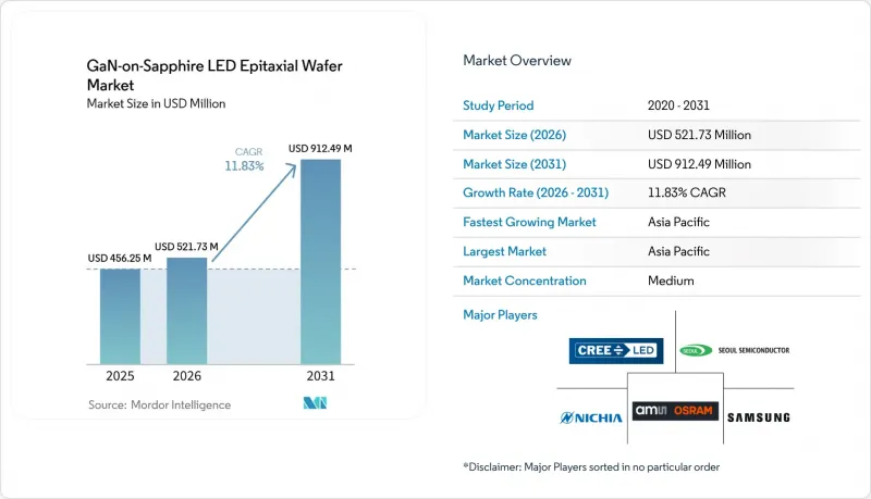
Mordor Intelligence에 의하면, GaN-on-사파이어 LED 에피텍셜 웨이퍼 시장 규모는 2025년 4억 5,625만 달러에서 2026년에는 5억 2,173만 달러로 확대되어 2031년까지 9억 1,249만 달러에 이를 것으로 예상되고 있어 2026년부터 2031년까지 CAGR 11.83%로 성장할 전망입니다.
본 보고서는 웨이퍼 직경(100mm 이하, 150mm, 200mm 이상), 용도(일반 조명, 자동차용 조명, 디스플레이 및 백라이트, 특수·산업용 조명) 및 지역별로 분류되어 있습니다. 시장 전망은 금액(달러) 기준으로 제시되어 있습니다.
전 세계 GaN-on-사파이어 LED 에피택셜 웨이퍼 시장 동향 및 인사이트
미니 LED 및 마이크로 LED 디스플레이의 보급 확대
현재 고급 TV 브랜드들은 패널 1장당 1만-2만 5천 개의 미니 LED 다이를 탑재하고 있으며, 엣지 라이트 방식의 백라이트로는 구현할 수 없는 2,000개 이상의 로컬 디밍 구역을 구현하고 있습니다. Ennostar의 2025년 합병을 통해 400대 이상의 금속 유기 화학 기상 증착(MOCVD) 반응기가 단일 공급망으로 통합됨에 따라, 애플과 삼성에 대한 웨이퍼 공급이 확보되었을 뿐만 아니라 에피택셜 공정의 관리도 강화되었습니다. PlayNitride와 Plessey는 사파이어 기반의 모노리식 마이크로 LED 어레이를 채택함으로써, 하이브리드형 실리콘 백플레인 방식에 수반되는 물질 이동으로 인한 수율 저하를 피하고, 이를 증강현실(AR) 헤드셋용 기술로 자리매김하고 있습니다. 자동차의 계기판도 1제곱미터당 10,000칸델라를 초과하며, 햇빛 아래에서도 식별 가능한 휘도를 구현하는 마이크로 LED 클러스터로 전환되고 있습니다. 이는 기존의 형광체 변환형 백색 LED가 열적 한계 내에서 충족하기 어려운 사양입니다. 이러한 기술들의 도입이 맞물려, 정밀한 파장 비닝과 낮은 순방향 전압 편차를 지원하는 균일한 GaN-on-sapphire 에피택셜 웨이퍼에 대한 지속적인 수요를 창출하고 있습니다.
형광체를 사용하지 않는 초고휘도 조명으로의 급속한 전환
건축용 및 원예용 조명 기구는 황색 형광체를 이용한 다운컨버전으로 인한 15-25%의 에너지 손실을 없애기 위해, 직접 발광형 적색·녹색·청색 클러스터 방식으로 전환되고 있습니다. 2024년에 발표된 조사에 따르면, 사파이어 상의 양자 우물에서 외부 양자 효율은 청색의 경우 52.4%, 녹색의 경우 25.2%에 달하며, 이는 2010년의 성능 벤치마크보다 약 2배 높은 수치입니다. 2025년 1월부터 시행되고 있는 유럽의 에코디자인 지침에서는 2027년까지 최소 광속 효율을 1와트당 210루멘으로 높일 것을 규정하고 있으며, 복잡한 열 관리가 필요 없이 이 목표를 달성할 수 있는 무형광체 어레이에 대한 관심이 높아지고 있습니다. 산안 옵토일렉트로닉스(San'an Optoelectronics)는 후베이성에서 추진 중인 116억 위안 규모의 확장 계획 중 40%를 원예용으로 최적화된 협대역 적색 및 녹색 다이 생산에 할당함으로써, 이러한 고휘도 소자에 대한 상업적 수요가 높음을 강조하고 있습니다. 규제 압력, 양자 우물의 효율 향상, 그리고 생산 능력 확대가 맞물리면서, 형광체를 사용하지 않는 조명은 사파이어 기판 위의 GaN 웨이퍼에 있어 지속적인 성장 동력으로서의 입지를 확고히 하고 있습니다.
200mm를 초과하는 크기의 경우 열팽창률 불일치로 인한 수율 저하
사파이어의 열팽창 계수(7.5×10??K?¹)와 질화갈륨의 열팽창 계수(5.6×10??K?¹)의 차이로 인해, 두께 5µ m을 초과하는 에피층에는 -1.0--1.5GPa의 잔류 압축 응력이 발생하여, 200 mm 웨이퍼에서 뒤틀림이나 균열의 발생률을 높이고 있습니다. 2024년 12월 나노소재에 관한 조사 결과, 200mm 사파이어 웨이퍼 상에서 GaN의 두께가 20µm을 초과하면 0.3cm?²를 넘는 거시 균열 밀도가 확인되었으며, 이러한 웨이퍼는 고출력 LED에 적합하지 않다는 사실이 밝혀졌습니다. 패턴화된 기판이나 순응성 AlN 버퍼층은 뒤틀림을 50µm 미만으로 억제할 수 있지만, 사이클 타임이 15-20% 증가하고 소모품 비용도 상승합니다. 따라서 디스플레이 제조업체들은 200mm 포맷이 면적 측면에서 78%의 우위를 차지함에도 불구하고, 미니 LED 백라이트용으로 계속해서 150mm 웨이퍼를 지정하고 있습니다. 응력 관리 기술이 성숙해지기 전까지는 웨이퍼 수준에서 경제성 측면에서 소경 제품이 더 유리하기 때문에 단기적인 전환 계획은 자제되고 있습니다.
부문별 분석
2025년, 150mm 포맷은 GaN-on-사파이어 LED 에피택셜 웨이퍼 시장 점유율의 48.78%를 차지했습니다. 이는 단위 면적당 처리량과 3×10?-5×10? cm?² 범위 내에 속하는 스레딩 전위 밀도 간의 균형을 반영한 것입니다. 자동차용 어댑티브 빔 모듈에서는 순방향 전압의 편차가 ±50 mV 이내로 유지되며, 킬로헤르츠급 구동 주파수에서도 열 예산을 관리 가능한 범위로 억제할 수 있기 때문에 이러한 균일성이 중요하게 여겨집니다. Ennostar사가 보유한 400대 이상의 MOCVD 장비는 여전히 150mm 사양입니다. 이는 단일 반응기를 200mm 사양으로 개조하는 데 200만-300만 달러의 비용이 소요되고, 이미 인증된 공정 흐름에 차질을 빚기 때문입니다. Veeco사의 Propel300 플랫폼은 8×150mm 구성으로 20%의 처리량을 실현하여 웨이퍼당 감가상각비를 절감하는 동시에, 대구경 웨이퍼의 비용 경쟁력을 확보하고 있습니다. 그 결과, 150mm 웨이퍼용 GaN-on-사파이어 LED 에피택셜 웨이퍼 시장 규모는 그 비중은 감소하겠지만, 예측 기간 중반까지는 여전히 주요 수익원으로 남아 있을 것으로 예측됩니다.
웨이퍼당 면적을 78% 늘리는 것을 목표로 하는 가운데, 200mm 이상의 웨이퍼 채택은 2031년까지 연평균 성장률(CAGR) 12.84%로 증가할 것으로 예측됩니다. 그러나 GaN의 두께가 20µm을 초과하면 잔류 압축 응력이 종종 -1.2GPa를 초과하고, 거시 균열의 밀도가 0.3cm?²를 넘어 증가합니다. 패턴화된 사파이어 기판과 컴플라이언트 AlN 버퍼는 뒤틀림을 50µm 미만으로 줄여주지만, 공정 시간을 15-20% 증가시키기 때문에 다이당 비용 절감 효과는 상쇄됩니다. 자외선 C(UVC) LED는 최대 100 mm 크기의 포맷을 사용할 수 있으며, 알루미늄 조성을 정밀하게 제어함으로써 휴대용 살균기용으로 265 nm에서 5% 이상의월플러그 효율을 달성하고 있습니다. 장비 공급업체는 5장 × 200mm 규모의 배치 처리를 지원하지만, 초기 도입 기업들로부터 특히 고출력 다이에서 결함으로 인한 불량품이 이론상의 비용 이점을 상당 부분 상쇄하고 있다는 보고가 있습니다. 수율 공학 분야에서 획기적인 진전이 나타나기 전까지는 구매자들이 성숙한 제품용으로는 150mm, 최첨단 디스플레이용으로는 200mm로 주문을 계속 분할할 것이기 때문에 GaN-on-사파이어 LED 에피택셜 웨이퍼 시장 점유율 변동은 제한적일 것으로 보입니다.
지역별 분석
2025년 현재, 아시아태평양은 전 세계 매출의 66.85%를 차지하고 있으며, 이 지역의 GaN-on-사파이어 LED 에피택셜 웨이퍼 시장은 2031년까지 연평균 성장률(CAGR) 12.75%로 성장할 것으로 전망됩니다. 대만이 수출의 중심지이며, Ennostar는 2025년 합병 이후 여러 거점에서 400대 이상의 금속 유기 화학 기상 증착(MOCVD) 장비를 가동하고 있습니다. 중국도 이러한 규모를 보완하고 있으며, San'an Optoelectronics는 2025년에 약 2,400만 장의 웨이퍼를 처리할 예정이며, 후베이성의 미니 LED 캠퍼스 확장을 위해 116억 위안을 투자하고 있습니다. 일본에서는 화합물 반도체 팹 비용의 최대 50%를 지원하는 보조금 프로그램이 닛야 화학공업의 사파이어 기판에 대한 수직 통합을 뒷받침하고 있으며, 이를 통해 해당 지역은 원자재 가격의 급등으로부터 보호받고 있습니다. 이러한 노력들이 맞물려, 예측 기간 동안 GaN-on-사파이어 LED 에피택셜 웨이퍼 시장 규모에서 아시아태평양의 우위가 유지될 것으로 전망됩니다.
북미에서는 ‘CHIPS and Science Act’에 따라 520억 달러가 국내 팹에 투자됨에 따라 다시 입지를 다지고 있습니다. Veeco Instruments는 2024년, 미국의 파워 일렉트로닉스 고객을 대상으로 첫 번째 Propel300 GaN 시스템을 출하하며, 새로운 에피택셜 생산 능력의 가동을 알렸습니다. 산안(San'an)이 루미레즈(Lumileds)를 2억 3,900만 달러에 인수하려는 계획은 북미 자동차 조명 계약을 중국공급망에 임베디드시킴으로써 해당 지역의 통합 수준을 한층 더 높이고 있습니다. 이러한 움직임으로 인해 2020년대 후반에는 해당 대륙의 GaN-on-사파이어 LED 에피택셜 웨이퍼 시장 점유율이 상승할 가능성이 있지만, 아시아산 기판 수입에 대한 의존도는 당분간 제약 요인으로 남아 있을 것입니다.
유럽은 2025년 매출에서 미미한 점유율에 그치고 있지만, 질화갈륨 및 실리콘카바이드 생산 라인에 자금을 배분하는 430억 유로 규모의 ‘칩스법’의 혜택을 받고 있습니다. 오스람(Osram)의 EVIYOS 적응형 빔 플랫폼은 프리미엄 웨이퍼 가격을 정당화할 수 있는 고부가가치 자동차용 다이 개발에 이 지역이 주력하고 있음을 상징합니다. 독일, 네덜란드, 프랑스의 수직 농업 프로젝트에서는 원예용 미니 LED 어레이가 채택되어 특수 용도 분야 수요를 주도하고 있습니다. 세계 기타 지역, 즉 라틴아메리카, 중동 및 아프리카는 여전히 개발도상국이지만, 자외선 C(UVC) 수처리 시범 사업이 기반을 다져가고 있으며, 이 분야에서 사파이어가 실리콘에 비해 갖는 열적 우위가 매우 중요합니다. 이러한 지역들은 전반적으로 판매량 증가에 기여하고 있지만, GaN-on-사파이어 LED 에피택셜 웨이퍼 시장에서 아시아태평양의 우위를 뒤집을 가능성은 거의 없을 것입니다.
기타 혜택:
- 엑셀 형식 시장 예측(ME) 시트
- 3개월간의 애널리스트 지원
자주 묻는 질문
목차
제1장 서론
제2장 조사 방법
제3장 주요 요약
제4장 시장 구도
제5장 시장 규모와 성장 예측
제6장 경쟁 구도
제7장 시장 기회와 향후 전망
JHSAccording to Mordor Intelligence, the gaN-on-Sapphire lED epitaxial wafer market size is expected to increase from USD 456.25 million in 2025 to USD 521.73 million in 2026 and reach USD 912.49 million by 2031, growing at a CAGR of 11.83% over 2026-2031.

This report is Segmented by Wafer Diameter (Up To 100 Mm, 150 Mm, 200 Mm and Above), Application (General Lighting, Automotive Lighting, Display and Backlighting, Specialty and Industrial Lighting), and Geography. The Market Forecasts are Provided in Terms of Value (USD).
Global GaN-on-Sapphire LED Epitaxial Wafer Market Trends and Insights
Increasing Penetration of Mini and Micro-LED Displays
Premium television brands now mount between 10,000 and 25,000 mini-LED dies per panel, unlocking more than 2,000 local-dimming zones that edge-lit backlights cannot match. Ennostar's 2025 merger integrated over 400 metal-organic chemical-vapor-deposition (MOCVD) reactors into a single supply chain, ensuring wafer availability for Apple and Samsung and tightening epitaxial process control. PlayNitride and Plessey use monolithic micro-LED arrays on sapphire to bypass the mass-transfer yield losses that plague hybrid silicon-backplane approaches, positioning their technology for augmented-reality headsets. Automotive cockpits are also shifting to micro-LED clusters that achieve daylight-readable luminance above 10,000 candelas per square meter, a specification conventional phosphor-converted white LEDs struggle to meet within thermal limits. Together, these deployments create sustained demand for uniform GaN-on-sapphire epitaxial wafers that support tight wavelength binning and low forward-voltage spread.
Rapid Shift Toward Phosphor-Free Ultra-High-Brightness Lighting
Architectural and horticultural fixtures are migrating to direct-emission red-green-blue clusters that eliminate the 15-25% energy loss from yellow-phosphor down-conversion. Research published in 2024 showed external quantum efficiencies reaching 52.4% for blue and 25.2% for green quantum wells on sapphire, roughly doubling 2010 performance benchmarks. Europe's Ecodesign Directive, active since January 2025, raises minimum efficacy to 210 lumens per watt by 2027, accelerating interest in phosphor-free arrays that meet the target without complex thermal management. San'an Optoelectronics earmarked 40% of its CNY 11.6 billion Hubei expansion for narrow-band red and green dies optimized for horticulture, underlining the commercial pull of these higher-brightness devices. The convergence of regulatory pressure, quantum-well efficiency gains, and capacity expansions positions phosphor-free lighting as a durable growth engine for GaN-on-sapphire wafers.
Thermal Mismatch-Driven Yield Losses Above 200 mm
Sapphire's thermal-expansion coefficient of 7.5 X 10⁻⁶ K-1 versus gallium-nitride's 5.6 X 10⁻⁶ K-1 induces residual compressive stress between -1.0 and -1.5 GPa in epilayers thicker than 5 µm, increasing bow and crack rates on 200 mm wafers. December 2024 Nanomaterials research documented macro-crack densities above 0.3 cm-2 when the GaN thickness exceeded 20 µm on 200 mm sapphire wafers, rendering such wafers unsuitable for high-power LEDs. Patterned substrates and compliant AlN buffers mitigate bow below 50 µm but add 15-20% cycle time and raise consumable costs. Display manufacturers, therefore, continue to specify 150 mm wafers for mini-LED backlights despite the 78% area advantage of 200 mm formats. Until stress-management techniques mature, wafer-level economics favor smaller diameters, tempering near-term transition plans.
Other drivers and restraints analyzed in the detailed report include:
- Cost Downward Trend in 150 mm GaN-on-Sapphire Wafers
- Government Incentives for Compound-Semiconductor Fabs
- Supply Constraints of High-Purity Sapphire Substrates
For complete list of drivers and restraints, kindly check the Table Of Contents.
Segment Analysis
The 150 mm format captured 48.78% of GaN-on-Sapphire LED Epitaxial Wafer market share in 2025, reflecting its balance between area throughput and threading-dislocation densities that stay within the 3 X 10⁸-5 X 108 cm-2 range. Automotive adaptive-beam modules value this uniformity because forward-voltage spread remains under +-50 mV, keeping thermal budgets manageable at kilohertz drive frequencies. Ennostar's fleet of more than 400 MOCVD chambers is still tooled for 150 mm, as retrofitting a single reactor to 200 mm costs USD 2-3 million and disrupts qualified process flows. Veeco's Propel300 platform delivers 20% throughput in its 8X150 mm configuration, reducing depreciation per wafer and locking in the cost advantage of the larger diameter. As a result, the GaN-on-Sapphire LED Epitaxial Wafer market size for 150 mm wafers is expected to remain the revenue anchor through the middle of the forecast window, even though its proportional share declines.
Adoption of 200 mm and larger wafers is projected to rise at a 12.84% CAGR to 2031 as display makers seek the 78% area gain per slice, yet residual compressive stress often exceeds -1.2 GPa and elevates macro-crack density beyond 0.3 cm-2 when GaN exceeds 20 µm. Patterned-sapphire substrates and compliant AlN buffers reduce bow below 50 µm but add 15-20% process time, muting the per-die savings. Up to 100 mm formats are available for ultraviolet-C LEDs, with tight control of aluminum composition enabling≥5% wall-plug efficiency at 265 nm for portable sterilizers. Equipment vendors support 5X200 mm batch loads, yet early adopters report that defect-attributed scrap negates much of the theoretical cost benefit, especially for high-power dies. Until yield-engineering breakthroughs emerge, buyers will continue to split orders between 150 mm for mature products and 200 mm for bleeding-edge displays, limiting abrupt share shifts within the GaN-on-Sapphire LED Epitaxial Wafer market.
Geography Analysis
Asia-Pacific accounted for 66.85% of global revenue in 2025, and the regional GaN-on-Sapphire LED Epitaxial Wafer market is projected to grow at a 12.75% CAGR through 2031. Taiwan anchors exports, with Ennostar operating more than 400 metal-organic chemical-vapor-deposition reactors across multiple sites after its 2025 merger. China complements this scale; San'an Optoelectronics processed about 24 million wafers in 2025 and is investing CNY 11.6 billion to ramp a Hubei mini-LED campus. Japan's subsidy program covering up to 50% of compound-semiconductor fab costs underpins Nichia's vertical move into sapphire substrates, helping shield the region from raw-material shocks. Together, these initiatives preserve Asia-Pacific's lead in the GaN-on-Sapphire LED Epitaxial Wafer market size over the forecast horizon.
North America is regaining footing as the CHIPS and Science Act channels USD 52 billion into domestic fabs. Veeco Instruments shipped its first Propel300 GaN system to a U.S. power-electronics customer in 2024, signaling the launch of fresh epitaxial capacity. San'an's planned USD 239 million acquisition of Lumileds folds North American automotive-lighting contracts into a Chinese supply chain, boosting the region's integration depth. These moves could lift the continent's GaN-on-Sapphire LED Epitaxial Wafer market share by the late 2020s, although reliance on Asian substrate imports remains a near-term constraint.
Europe captured a modest slice of 2025 revenue but benefits from the EUR 43 billion Chips Act, which allocates funds for gallium nitride and silicon carbide lines. Osram's EVIYOS adaptive-beam platform exemplifies the region's focus on high-value automotive dies that justify premium wafer pricing. Vertical-farming projects across Germany, the Netherlands, and France are adopting horticultural mini-LED arrays, driving specialty demand. The rest of the World, Latin America, the Middle East, and Africa remain nascent, yet pilot ultraviolet-C water-treatment schemes are creating beachheads where sapphire's thermal advantage over silicon is critical. Collectively, these pockets contribute incremental volume but are unlikely to displace Asia-Pacific's dominance in the GaN-on-Sapphire LED Epitaxial Wafer market.
- Nichia Corporation
- Osram Opto Semiconductors GmbH
- Cree LED, Inc.
- Samsung LED Co., Ltd.
- Seoul Semiconductor Co., Ltd.
- Epistar Corporation
- San'an Optoelectronics Co., Ltd.
- HC SemiTek Corporation
- Plessey Semiconductors Ltd.
- LG Innotek Co., Ltd.
- Lumileds Holding B.V.
- Bridgelux, Inc.
- Lextar Electronics Corp.
- Silanna Semiconductor Pty Ltd.
- Aledia SA
- Opto Tech Corporation
- PlayNitride Inc.
- Tianma Microelectronics Co., Ltd.
- Innolux Corporation
- Veeco Instruments Inc.
Additional Benefits:
- The market estimate (ME) sheet in Excel format
- 3 months of analyst support
TABLE OF CONTENTS
1 INTRODUCTION
- 1.1 Study Assumptions and Market Definition
- 1.2 Scope of the Study
2 RESEARCH METHODOLOGY
3 EXECUTIVE SUMMARY
4 MARKET LANDSCAPE
- 4.1 Market Drivers
- 4.1.1 Increasing Penetration of Mini and Micro-LED Displays
- 4.1.2 Rapid Shift Toward Phosphor-Free Ultra-High-Brightness Lighting
- 4.1.3 Cost Downward Trend in 150 mm GaN-on-Sapphire Wafers
- 4.1.4 Government Incentives for Compound-Semiconductor Fabs
- 4.1.5 Adoption of GaN Epilayers for UV-C Sterilization LEDs
- 4.1.6 Integration of GaN LEDs in Li-Fi Optical Communications
- 4.2 Market Restraints
- 4.2.1 Thermal Mismatch-Driven Yield Losses Above 200 mm
- 4.2.2 Supply Constraints of High-Purity Sapphire Substrates
- 4.2.3 Capital-Intensive MOCVD Tooling for Uniform Thick GaN Layers
- 4.2.4 Competition from Emerging GaN-on-Si Platforms in TV Backlighting
- 4.3 Industrial Analysis
- 4.4 Impact of Macroeconomic Factors on the Market
- 4.5 Technology Analysis
- 4.6 Porter's Five Forces Analysis
- 4.6.1 Bargaining Power of Suppliers
- 4.6.2 Bargaining Power of Buyers
- 4.6.3 Threat of New Entrants
- 4.6.4 Threat of Substitutes
- 4.6.5 Intensity of Competitive Rivalry
5 MARKET SIZE AND GROWTH FORECASTS (VALUE)
- 5.1 By Wafer Diameter
- 5.1.1 Upto 100 mm
- 5.1.2 150 mm
- 5.1.3 200 mm and Above
- 5.2 By Application
- 5.2.1 General Lighting
- 5.2.2 Automotive Lighting
- 5.2.3 Display and Backlighting
- 5.2.4 Specialty and Industrial Lighting
- 5.3 By Geography
- 5.3.1 North America
- 5.3.2 Europe
- 5.3.3 Asia-Pacific
- 5.3.4 Rest of the World
6 COMPETITIVE LANDSCAPE
- 6.1 Market Concentration
- 6.2 Strategic Moves
- 6.3 Market Share Analysis
- 6.4 Company Profiles (includes Global Level Overview, Market Level Overview, Core Segments, Financials as available, Strategic Information, Market Rank/Share, Products and Services, Recent Developments)
- 6.4.1 Nichia Corporation
- 6.4.2 Osram Opto Semiconductors GmbH
- 6.4.3 Cree LED, Inc.
- 6.4.4 Samsung LED Co., Ltd.
- 6.4.5 Seoul Semiconductor Co., Ltd.
- 6.4.6 Epistar Corporation
- 6.4.7 San'an Optoelectronics Co., Ltd.
- 6.4.8 HC SemiTek Corporation
- 6.4.9 Plessey Semiconductors Ltd.
- 6.4.10 LG Innotek Co., Ltd.
- 6.4.11 Lumileds Holding B.V.
- 6.4.12 Bridgelux, Inc.
- 6.4.13 Lextar Electronics Corp.
- 6.4.14 Silanna Semiconductor Pty Ltd.
- 6.4.15 Aledia SA
- 6.4.16 Opto Tech Corporation
- 6.4.17 PlayNitride Inc.
- 6.4.18 Tianma Microelectronics Co., Ltd.
- 6.4.19 Innolux Corporation
- 6.4.20 Veeco Instruments Inc.
7 MARKET OPPORTUNITIES AND FUTURE OUTLOOK
- 7.1 White-Space and Unmet-Need Assessment
