
|
시장보고서
상품코드
2063439
AlGaN 심자외선 LED 에피텍셜 웨이퍼 시장 : 점유율 분석, 업계 동향과 통계, 성장 예측(2026-2031년)AlGaN Deep-UV LED Epitaxial Wafer - Market Share Analysis, Industry Trends & Statistics, Growth Forecasts (2026 - 2031) |
||||||
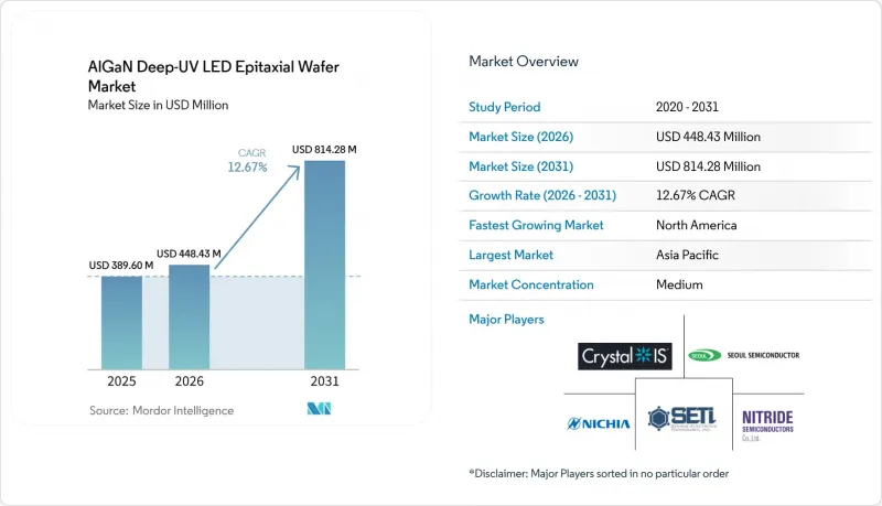
Mordor Intelligence에 의하면, AlGaN 심자외선 LED 에피텍셜 웨이퍼 시장 규모는 2025년 3억 8,960만 달러, 2026년 4억 4,843만 달러에서 2031년까지 8억 1,428만 달러로 확대되어 2026년부터 2031년까지 사이에 CAGR 12.67%를 나타낼 것으로 예측됩니다.
본 보고서는 기판 플랫폼(사파이어, AlN 템플릿 등), 파장대(UV-A(315-400 nm), UV-B(280-315 nm) 등), 웨이퍼 직경(100 mm 이하, 150 mm, 200 mm 이상), 용도(물 및 공기 소독, 표면 멸균, 의료 및 헬스케어 기기 등), 그리고 지역별로 분류되어 있습니다. 시장 전망은 금액(달러) 기준으로 제시되어 있습니다.
전 세계 AlGaN 심자외선 LED 에피택셜 웨이퍼 시장 동향 및 분석
수은 UV 램프에 대한 규제상 금지 조치
유럽연합(EU)에서 2025년 12월까지 수은 함유 램프를 단계적으로 폐지해야 하는 의무와 2027년 2월에 종료되는 RoHS의 최종 적용 제외 조치로 인해, 유틸리티체와 OEM 업체들은 솔리드 스테이트 모듈을 도입할 수밖에 없는 상황에 놓여 있습니다. 미나마타 협약은 세계적 기준을 강화함으로써, 수출 주도형 아시아 제조 거점에서도 이 협약을 채택하도록 하는 압력을 확실히 하고 있습니다. 2025년 11월에 시작된 닛야 화학공업의 무수은 소독 이니셔티브는 수직 통합형 공급업체가 이 이니셔티브를 준수하기 위해 내부 업무를 재편하고 있는 실제 사례를 보여주고 있습니다. 단기적인 도입은 개조 비용이 제한적인 100W 미만의 말단 이용 시스템에 집중되어 있지만, 메가와트 규모의 지자체에 의한 설비 교체는 여전히 막대한 투자가 필요합니다. 그 결과, AlGaN 심자외선 LED 에피택셜 웨이퍼 시장의 조달 사이클은 산업용 개조 분야로 확산되기 전에, 주거용 및 휴대용 기기에 우선적으로 집중되고 있습니다.
사용 현장에서의 물 소독에 대한 수요 증가
수돗물이나 Off-grid 환경에서 병원체에 대한 우려가 커지면서, 265-280 nm 파장의 LED를 탑재한 소형 UV-C 정수기 수요가 증가하고 있습니다. AlGaN 에피택셜 웨이퍼를 기반으로 한 칩 온 보드(COB) 모듈은 현재 5.2 mm² 미만의 패키지에서 275 nm 파장 시 145 mW의 출력을 구현하고 있어, 배터리 구동 방식의 설계를 가능하게 하고 있습니다. ‘끓는 물 주의보’가 발령된 아시아·태평양 지역의 가정들이 초기 도입자로 나서고 있으며, 재난 구호 기관들도 현장 투입용으로 경량 LED 장치를 지정하고 있습니다. 각 정수기에는 여러 개의 칩이 통합되어 있어 40 mJ/cm²의 조사량을 실현하므로, 다이 크기가 작음에도 불구하고 웨이퍼 소비량을 줄일 수 있습니다. 생산량이 증가함에 따라 웨이퍼 제조업체들은 100mm 사파이어 웨이퍼의 처리 능력을 최적화하고 있으며, 이로 인해 중출력 부문에서 AlN 템플릿에 도전할 수 있는 비용 하한선이 형성되고 있습니다.
수은 램프에 비해 와트당 제조 비용이 높습니다.
수 메가와트 규모에서는 UV-C LED 시스템의 비용이 여전히 기존의 수은 램프에 비해 와트당 2-4배 더 비싸며, 예산에 제약이 있는 유틸리티체의 경우 투자 회수 기간이 7년 이상에 달하고 있습니다. 에피택셜 웨이퍼 비용이 디바이스 비용의 거의 절반을 차지하기 때문에 EQE(외부 양자 효율)가 조금만 향상되어도 모듈 가격을 직접 낮출 수 있습니다. 니치아 화학공업의 2024년 12월 기준 280nm 디바이스는 월플러그 효율 7.4%를 달성했으나, 여전히 고급 소독 용도의 틈새 시장을 타겟으로 하고 있어 일반 지자체에서의 대규모 도입과는 여전히 거리가 있다는 점이 부각되고 있습니다. 이익률이 낮은 아시아태평양의 전력 회사들은 웨이퍼 가격이 하락하거나 보조금을 받을 수 있게 될 때까지 대규모 전환을 미루고 있습니다. 따라서 AlGaN 심자외선 LED 에피택셜 웨이퍼 시장에서 이러한 제약은 단기적으로 가장 심각한 문제로 대두되고 있습니다.
부문별 분석
AlGaN 심자외선 LED 에피택셜 웨이퍼 시장은 2025년에 2억 3,000만 달러에 달하며 58.19%의 점유율을 차지한 반면, AlN 템플릿은 연평균 성장률(CAGR) 13.28%로 확대되어 2031년까지 2억 6,000만 미달러 이상의 매출 기여를 가져올 것으로 예측됩니다. CAGR 사파이어가 우위를 유지하고 있는 이유는 공급 체계, 반응로 레시피, 그리고 유리한 가격 책정이 성숙 단계에 이르렀기 때문이지만, 그 높은 스레딩 전위 밀도가 심자외선 효율을 저하시키고 있습니다. 한편, AlN의 격자 정합 성장을 통해 결함 밀도를 10? cm?² 미만으로 낮출 수 있었으며, 20-30%에 달하는 일관된 EQE(양자 효율) 향상을 실현하고 있습니다. 2026년 2월 HexaTech가 3인치 AlN을 출시했고, 2024년 6월에는 Crystal IS가 100mm 웨이퍼에서 99%의 유효 면적을 달성한 것은 규모 확대의 추세를 보여주고 있습니다.
파장별 전환 상황은 균일하지 않습니다. UV-A 및 UV-B 소자는 알루미늄 함량이 낮고 결함에 대한 내성이 있어 사파이어를 계속 사용하고 있지만, 270 nm 이하의 UV-C의 경우 실용적인 출력 수준을 달성하기 위해 AlN 템플릿의 채택이 점점 더 필수적이 되고 있습니다. 웨이퍼 제조업체들이 현재의 100mm 블랭크보다 다이당 비용을 30% 절감할 수 있을 것으로 기대되는 150mm AlN 라인의 준비를 진행함에 따라, 비용 차이는 점차 줄어들고 있습니다. 이것이 성공한다면, AlGaN 심자외선 LED 에피택셜 웨이퍼 시장 전반에서 조달 전략이 재검토될 것이며, 수직 통합형 기업들은 지적 재산권과 이익률을 지키기 위해 AlN 성장 공정을 자체 생산하게 될 것입니다.
UV-C용 웨이퍼는 2025년에 매출의 46.14%(1억 8,000만 달러)를 차지하며, 연평균 성장률(CAGR) 13.86%로 급성장하고 있습니다. 이 살균 최적 파장인 265nm는 물, 공기 및 표면의 살균 기준을 충족합니다. 니치아 화학공업이 700mA에서 263mW를 출력하는 280nm 칩의 양산을 확대한 것은 상용화 준비가 완료되었음을 보여줍니다. UV-A는 경화 처리 및 위조품 감지를 주요 용도로 하며, 35% 이상의 높은 양자 효율(EQE)을 자랑하지만, 램프 시장이 성숙기에 접어들었기 때문에 출하량 증가세는 완만합니다. UV-B는 피부과 치료와 원예에 도움을 주고 있습니다. 규제 당국의 승인이 사업 규모 확대에 제약 요인으로 작용하고 있지만, 높은 가격 책정을 통해 판매량 감소를 상쇄하고 있습니다.
240 nm 이하의 원자외선(Far-UVC)은 여전히 연구 개발의 최전선입니다. Silanna UV사는 방사 강도를 2 mW/sr로 두 배로 높인 233 nm 장치를 개발하여, 향후 공간 소독의 가능성을 시사하고 있습니다. 그러나 알루미늄 함유율이 60%를 초과하면 변형이나 결함에 대한 민감도가 높아져 수율 저하를 초래하고 있습니다. 전반적으로, 파장별 세분화는 용도별 수요를 반영하고 있습니다. 소독 용도가 UV-C 수요를 견인하는 한편, 산업용 센서가 틈새 시장인 원자외선(far-UVC)의 생산량을 끌어올리고 있으며, 이러한 요인들이 결합되어 AlGaN 심자외선 LED 에피택셜 웨이퍼 시장의 설계 사양을 형성하고 있습니다.
지역별 분석
아시아태평양에서는 2025년에 AlGaN 심자외선 LED 에피택셜 웨이퍼의 매출액이 2억 2,000만 달러에 달하고, 전 세계 수요의 55.83%를 차지했습니다. 이는 주로 수직 통합형인 일본 및 한국공급업체들이 기판 성장, 에피택시, 디바이스 패키징 분야를 장악하고 있기 때문입니다. 니치아 화학공업이나 닛키소 등 일본 제조업체들은 수십 년에 걸친 MOCVD 노하우를 활용하는 한편, 한국 기업들은 광범위한 특허 포트폴리오를 활용하여 가전제품 및 수처리 기기 OEM 제조업체들과 장기 계약을 확보하고 있습니다. 중국의 국내 반도체 전략도 화합물 반도체 라인에 자본을 투입하고 있지만, MOCVD 장비 및 전구체 가스에 대한 수출 규제로 인해 고성능 UV-C 웨이퍼의 양산화는 여전히 지연되고 있습니다. 또한, 이 지역에서는 패턴화 사파이어 및 AlN 기판에 대한 정부의 지원 조치가 시행되고 있으며, 이를 통해 팹은 해외 경쟁사들에 비해 비용 면에서 즉각적인 우위를 점하고 있습니다. 그 결과, 적어도 2028년까지는 아시아·태평양 지역이 AlGaN 심자외선 LED 에피택셜 웨이퍼 시장의 주요 생산 거점으로 남을 것으로 전망됩니다.
북미에서는 2025년 매출이 9,000만 달러를 기록하고, 2031년까지 연평균 성장률(CAGR) 12.93%로 성장할 전망입니다. 이는 CHIPS법에 따라 새로운 AlN 기판 공장, 반응기 설비 및 후공정 패키징 라인에 자금이 지원되고 있기 때문입니다. 의료 및 항공우주 산업의 국내 구매업체들은 FDA 및 IEC 안전 기준을 충족하는 고신뢰성 UV-C 장치를 찾고 있으며, 공급망 리스크를 줄이기 위해 현지 조달을 촉진하고 있습니다. 미국의 여러 팹에서는 GaN 파워 디바이스 생산 라인에서 전용한 200mm MOCVD 리액터의 개조를 진행 중이며, 이를 통해 인증 절차 기간 단축과 다이당 비용 절감이 가속화되고 있습니다. 연구 중심 대학과 국립 연구소는 터널 접합 및 원자외선(far-UVC) 개발을 위한 계측 기술 지원을 제공하며, 독자적인 공정 레시피 파이프라인을 구축하고 있습니다. 이러한 생태계의 연계를 통해, 예측 기간 동안 북미는 고사양 웨이퍼의 지역별 구매자 중 가장 빠른 성장세를 보일 것으로 전망됩니다.
유럽에서 시장 점유율은 작지만, 수은 램프에 대한 엄격한 금지 조치로 인해 지자체 상수도 시설 전반에 걸쳐 솔리드 스테이트 방식으로의 개조가 진행되고 있어, 그 혜택을 누리고 있습니다. 독일과 프랑스는 국가 혁신 기금을 통해 화합물 반도체의 시범 생산 라인을 지원하고 있지만, 밸류체인의 분절화로 인해 규모의 경제 효과가 제한되고 있습니다. 세계 기타 지역(ROW) 수요는 현지 생산 능력이 제한적이고 수입 모듈에 대한 의존도가 높기 때문에 여전히 초기 단계에 머물러 있습니다. 그러나 비용 효율성이 개선된다면, 걸프 연안 국가들의 해수 담수화 프로젝트나 남미의 휴대용 소독 장치가 조기 도입 사례로 부상할 것입니다. 전 세계 각국 정부의 주도 하에 국내 웨이퍼 생산을 촉진하는 프로그램이 확대됨에 따라, 지역별 전문화가 진행되면서 AlGaN 심자외선 LED 에피택셜 웨이퍼 시장의 거래 패턴이 재편되고 있습니다.
기타 혜택:
- 엑셀 형식 시장 예측(ME) 시트
- 3개월간의 애널리스트 지원
자주 묻는 질문
목차
제1장 서론
제2장 조사 방법
제3장 주요 요약
제4장 시장 구도
제5장 시장 규모와 성장 예측
제6장 경쟁 구도
제7장 시장 기회와 향후 전망
JHSAccording to Mordor Intelligence, the alGaN deep-UV lED epitaxial wafer market size is projected to expand from USD 389.60 million in 2025 and USD 448.43 million in 2026 to USD 814.28 million by 2031, registering a CAGR of 12.67% between 2026 to 2031.

This report is Segmented by Substrate Platform (Sapphire, Aln Template, and More), Wavelength Band (UV-A (315-400 Nm), UV-B (280-315 Nm), and More), Wafer Diameter (Up To 100 Mm, 150 Mm, 200 Mm and Above), Application (Water and Air Disinfection, Surface Sterilisation, Medical and Healthcare Devices, and More), and Geography. The Market Forecasts are Provided in Terms of Value (USD).
Global AlGaN Deep-UV LED Epitaxial Wafer Market Trends and Insights
Regulatory Bans on Mercury UV Lamps
Mandatory phase-outs of mercury-containing lamps in the European Union by December 2025 and the final RoHS exemption ending in February 2027 compel utilities and OEMs to adopt solid-state modules. The Minamata Convention reinforces the global baseline, ensuring adoption pressure even in export-driven Asian manufacturing hubs. Nichia's mercury-free disinfection initiative, launched in November 2025, demonstrates how vertically integrated suppliers are realigning internal operations to comply with the initiative. Near-term deployments concentrate on point-of-use systems below 100 W where retrofit costs are limited, while megawatt-scale municipal upgrades remain capital-intensive. Consequently, procurement cycles for the AlGaN deep-UV LED epitaxial wafer market are front-loaded into residential and portable devices before cascading into industrial retrofits.
Growing Demand for Point-of-Use Water Disinfection
Rising concerns about pathogens in tap water and in off-grid settings are fueling demand for compact UV-C purifiers powered by 265-280 nm LEDs. Chip-on-board modules based on AlGaN epitaxial wafers now deliver 145 mW at 275 nm in packages under 5.2 mm2, enabling battery-powered designs. Asia-Pacific households facing boil-water advisories are early adopters, and disaster-relief agencies specify lightweight LED units for field deployment. Each purifier integrates multiple chips to deliver 40 mJ/cm2 doses, thereby reducing wafer consumption despite smaller die sizes. As volumes rise, wafer producers optimize reactor throughput for 100 mm sapphire runs, creating a cost floor that challenges AlN templates in mid-power segments.
High USD/W Output Cost Versus Mercury Lamps
At multimegawatt scales, UV-C LED systems still cost two-to-four times more per watt than legacy mercury lamps, lengthening payback to over seven years in budget-constrained utilities. Epitaxial wafer costs account for nearly half of device costs, so every incremental gain in EQE directly lowers module pricing. Nichia's December 2024 280 nm device hit 7.4% wall-plug efficiency yet remains targeted at premium disinfection niches, highlighting the gap to mass municipal adoption. Asia-Pacific utilities, operating on tight margins, postpone large-scale conversions until wafer prices fall or subsidies become available. The constraint is therefore most severe in the near term for the AlGaN deep-UV LED epitaxial wafer market.
Other drivers and restraints analyzed in the detailed report include:
- Tunnel-Junction Designs Lowering Forward Voltage
- Patterned Sapphire Substrates Optimized for UVC
- Low EQE at 250-270 nm
For complete list of drivers and restraints, kindly check the Table Of Contents.
Segment Analysis
The AlGaN deep-UV LED epitaxial wafer market, attributed to sapphire, reached USD 0.23 billion in 2025, accounting for 58.19% share, while AlN templates are projected to expand at a 13.28% CAGR, lifting their revenue contribution to more than USD 0.26 billion by 2031. Sapphire's dominance stems from mature supply, reactor recipes, and favorable pricing, yet its high threading-dislocation density suppresses deep-UV efficiency. AlN's lattice-matched growth slashes defect density below 106 cm-2, yielding consistent EQE improvements of 20-30%. HexaTech's launch of 3-inch AlN in February 2026 and Crystal IS achieving 99% usable area on 100 mm wafers in June 2024 signpost scale-up momentum.
Migration is uneven across wavelengths. UV-A and UV-B devices retain sapphire because their lower aluminum content tolerates defects, whereas UV-C below 270 nm increasingly mandates AlN templates to attain usable power levels. Cost differentials are narrowing as wafer makers prepare 150 mm AlN lines that promise a 30% lower cost per die than today's 100 mm blanks. Success will recalibrate sourcing strategies across the AlGaN deep-UV LED epitaxial wafer market, with vertically integrated players internalizing AlN growth to protect intellectual property and margins.
UV-C wafers generated 46.14% revenue or USD 0.18 billion in 2025 and are accelerating at a 13.86% CAGR. Their germicidal peak at 265 nm aligns with water, air, and surface sterilization standards. Nichia's mass-production ramp of 280 nm chips delivering 263 mW at 700 mA underscores commercial readiness. UV-A targets curing and counterfeit detection, enjoying higher EQE above 35% but slower volume growth due to mature lamp competition. UV-B supports dermatological therapy and horticulture; regulatory approvals constrain scaling, yet premium pricing offsets lower unit counts.
Far-UVC below 240 nm remains a frontier in R&D. Silanna UV advanced 233 nm devices that double radiant intensity to 2 mW/sr, hinting at future occupied-space disinfection. However, aluminum fractions above 60% elevate strain and defect sensitivity, hindering yields. Overall, wavelength segmentation reflects application pull: disinfection drives UV-C demand while industrial sensors push niche far-UVC volumes, collectively shaping design specs within the AlGaN deep-UV LED epitaxial wafer market.
Geography Analysis
Asia-Pacific generated USD 0.22 billion in AlGaN deep-UV LED epitaxial wafer revenue in 2025, accounting for 55.83% of global demand, largely because vertically integrated Japanese and South Korean suppliers control substrate growth, epitaxy, and device packaging. Japanese producers such as Nichia and Nikkiso capitalize on decades of MOCVD know-how, while South Korean firms leverage expansive patent portfolios to secure long-term contracts with consumer-electronics and water-treatment OEMs. China's domestic semiconductor strategy also injects capital into compound-semiconductor lines, yet export controls on MOCVD tools and precursor gases continue to delay volume ramps for high-performance UV-C wafers. The region further benefits from government incentives that subsidize patterned-sapphire and AlN substrates, giving fabs an immediate cost advantage over overseas rivals. As a result, Asia-Pacific remains the primary manufacturing hub for the AlGaN deep-UV LED epitaxial wafer market through at least 2028.
North America recorded USD 0.09 billion in 2025 sales and is poised for a 12.93% CAGR through 2031, as the CHIPS Act provides funding for new AlN-substrate plants, reactor installations, and backend packaging lines. Domestic buyers in the medical and aerospace industries demand high-reliability UV-C devices that meet FDA and IEC safety criteria, encouraging local sourcing to reduce supply-chain risk. Several U.S. fabs are retrofitting 200 mm MOCVD reactors borrowed from GaN power-device lines, accelerating qualification timelines and lowering per-die costs. Research universities and national labs provide metrology support for tunnel-junction and far-UVC development, feeding a pipeline of proprietary process recipes. This ecosystem alignment positions North America as the fastest-growing regional buyer of high-specification wafers during the forecast window.
Europe commands a smaller share yet benefits from stringent mercury-lamp bans that drive solid-state retrofits across municipal water facilities. Germany and France support compound-semiconductor pilot lines through national innovation funds, but fragmented value chains limit economies of scale. Rest-of-World demand spanning the Middle East, Africa, and Latin America remains nascent, constrained by limited local manufacturing and reliance on imported modules. However, desalination projects in the Gulf and portable disinfection devices in South America are emerging as early adopters once cost parity improves. As sovereign programs worldwide encourage domestic wafer output, regional specialization intensifies, reshaping trading patterns within the AlGaN deep-UV LED epitaxial wafer market.
- Nitride Semiconductors Co., Ltd.
- Seoul Viosys Co., Ltd.
- Nichia Corporation
- Crystal IS, Inc.
- Sensor Electronic Technology, Inc.
- HexaTech, Inc.
- KYOCERA SLD Laser, Inc.
- Nikkiso Co., Ltd.
- ROHM Co., Ltd.
- Stanley Electric Co., Ltd.
- OSRAM GmbH
- Harvatek Corporation
- Luminus Devices, Inc.
- Silanna UV Pty. Ltd.
- LG Innotek Co., Ltd.
- Panasonic Industrial Devices SUNX Co., Ltd.
- Xiaomi Corporation (subsidiary Yeelight)
- Bolb Inc.
- Dowa Holdings Co., Ltd.
- Azzurro Semiconductors AG
Additional Benefits:
- The market estimate (ME) sheet in Excel format
- 3 months of analyst support
TABLE OF CONTENTS
1 INTRODUCTION
- 1.1 Study Assumptions and Market Definition
- 1.2 Scope of the Study
2 RESEARCH METHODOLOGY
3 EXECUTIVE SUMMARY
4 MARKET LANDSCAPE
- 4.1 Market Overview
- 4.2 Market Drivers
- 4.2.1 Regulatory Bans on Mercury UV Lamps
- 4.2.2 Growing Demand for Point-of-Use Water Disinfection
- 4.2.3 Tunnel-Junction Designs Lowering Forward Voltage
- 4.2.4 Patterned Sapphire Substrates Optimised for UVC
- 4.2.5 Integration into Semiconductor Lithography Tools
- 4.2.6 Sovereignty Programmes Funding Domestic DUV Fabs
- 4.3 Market Restraints
- 4.3.1 High USD/W Output Cost Versus Mercury Lamps
- 4.3.2 Low EQE at 250-270 nm
- 4.3.3 Thermal Management Limits of Flip-Chip Layouts
- 4.3.4 Limited Availability of Bulk AlN Substrates
- 4.4 Industry Analysis
- 4.5 Technological Outlook
- 4.6 Impact of Macroeconomic Factors
- 4.7 Porter's Five Forces Analysis
- 4.7.1 Bargaining Power of Suppliers
- 4.7.2 Bargaining Power of Buyers
- 4.7.3 Threat of New Entrants
- 4.7.4 Threat of Substitutes
- 4.7.5 Intensity of Competitive Rivalry
5 MARKET SIZE AND GROWTH FORECASTS (VALUE)
- 5.1 By Substrate Platform
- 5.1.1 Sapphire
- 5.1.2 AlN Template
- 5.1.3 Silicon Carbide (SiC)
- 5.1.4 Other Substrate Platforms
- 5.2 By Wavelength Band
- 5.2.1 UV-A (315-400 nm)
- 5.2.2 UV-B (280-315 nm)
- 5.2.3 UV-C (200-280 nm)
- 5.3 By Wafer Diameter
- 5.3.1 Up to 100 mm
- 5.3.2 150 mm
- 5.3.3 200 mm and Above
- 5.4 By Application
- 5.4.1 Water and Air Disinfection
- 5.4.2 Surface Sterilisation
- 5.4.3 Medical and Healthcare Devices
- 5.4.4 Industrial and Analytical Instruments
- 5.5 By Geography
- 5.5.1 North America
- 5.5.2 Europe
- 5.5.3 Asia-Pacific
- 5.5.4 Rest of the World
6 COMPETITIVE LANDSCAPE
- 6.1 Market Concentration
- 6.2 Strategic Moves
- 6.3 Market Share Analysis
- 6.4 Company Profiles (includes Global Level Overview, Market Level Overview, Core Segments, Financials as available, Strategic Information, Market Rank/Share, Products and Services, Recent Developments)
- 6.4.1 Nitride Semiconductors Co., Ltd.
- 6.4.2 Seoul Viosys Co., Ltd.
- 6.4.3 Nichia Corporation
- 6.4.4 Crystal IS, Inc.
- 6.4.5 Sensor Electronic Technology, Inc.
- 6.4.6 HexaTech, Inc.
- 6.4.7 KYOCERA SLD Laser, Inc.
- 6.4.8 Nikkiso Co., Ltd.
- 6.4.9 ROHM Co., Ltd.
- 6.4.10 Stanley Electric Co., Ltd.
- 6.4.11 OSRAM GmbH
- 6.4.12 Harvatek Corporation
- 6.4.13 Luminus Devices, Inc.
- 6.4.14 Silanna UV Pty. Ltd.
- 6.4.15 LG Innotek Co., Ltd.
- 6.4.16 Panasonic Industrial Devices SUNX Co., Ltd.
- 6.4.17 Xiaomi Corporation (subsidiary Yeelight)
- 6.4.18 Bolb Inc.
- 6.4.19 Dowa Holdings Co., Ltd.
- 6.4.20 Azzurro Semiconductors AG
7 MARKET OPPORTUNITIES AND FUTURE OUTLOOK
- 7.1 White-space and Unmet-need Assessment
